
Tungsten wafer probe is specifically designed for wafer testing during the production of integrated circuit. Wherein, wafer testing is to test each die on the chip. In the general, a probe made of tungsten material is mounted on the detection head, and contacts the contacts on the dies to test their electrical characteristics. Unqualified dies will be marked. Then, when the chip is cut into individual dies, these unqualified dies marked will be eliminated, and the next process will not be carried out, so as not to increase the manufacturing cost.
More details, please visit:
http://tungsten.com.cn/tungsten-needles.html
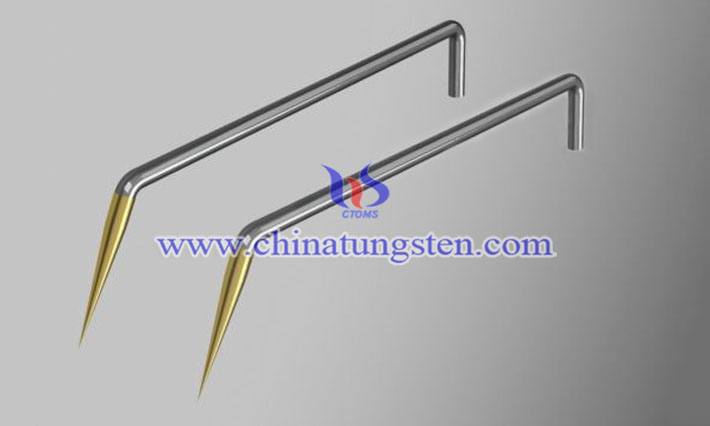
It means that the quality of tungsten wafer probe will greatly affect the good rate and efficiency of the integrated circuits produced.
In addition, the tungsten needle is tapered, it wears out after many times of tests, to a certain extent, the needle becomes thick to affect the accuracy of the test results, then you need to replace the tungsten needle. That is to say, tungsten probe is a consumable during wafer testing.


